Basic Logic Building Blocks
Multiplexors
- connects one of many inputs to one output
- n select lines for 2^n inputs

The simplest mux is a 2:1 mux:

A 4:1 mux looks like this:

General Mux

Implementing Logic Functions Using Muxes

We can do better than the previous example.
The following example implements a 3-input function using a 4:1 mux.

- could build circuit using any two of {a,b,c} as select inputs
Decoders
- inverse of multiplexor
- sets one ouput line (minterm) to one

- can implement logic functions
- good for multiple functions of same variable
- impractical for function with large # of inputs

- memory element

- implement by simple modifications to coupled inverters

- transform to obtain NAND and NOR implementations


- add clock to latch
- make latch state insensitive to input during low clock
- level sensitive latch

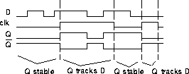
- example using timing diagram

Flip-Flops
- want instantaneous 'sample-and-keep'
- two level-sensitive latches with complementary clocks

- master-slave flip-flop or edge triggered
- negative or positive edge-trigger
- timing diagram

- building block for synchronous circuits
Ripple Counters
- store count, add one every clock cycle
- synchronous circuit
- begin with half adder
- Cout from bit n becomes Cin for bit n+1.
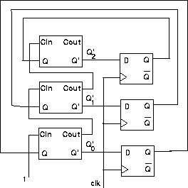
Cin carry in Qn bit n of the count --- Qn' + Cout - A 3-bit counter could thus be designed as follows:

In order to obtain a continuosly increasing count, we can unfortunately not simply connect the count+1 wires to the count wires. A clocked circuit will make things in operate correctly:

The clock period should be long enough to allow the value of count+1 to settle to their new values. A clock edge then simultaneously loads the latches with their new values, thereby starting the next cycle.
In order to finish the counter design, we need only design the details of the half-adder circuit. The truth table is as follows:
  Cin Qn | Cout Qn'
 -----------------
   0  0  |  0   0
   0  1  |  0   1
   1  0  |  0   1
   1  1  |  1   0

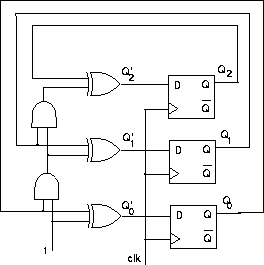
Cout = Cin AND Qn
Qn'  = Cin XOR Qn
The final counter design looks as follows:


Registers
Registers are a set of latches or flip-flops that are used
to store binary data. The following example shows a register
which either retains its value (load=0) or loads a value
from external inputs (load=1) on a clock edge. The design
for this register also illustrates a useful circuit design rule:
avoid modifying the path of the clock signal.

Shift Registers
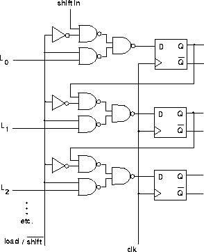
The following shift register design could be used to perform
serial-to-parallel or parallel-to-serial conversion.
